Semiconductor & Hi-Tech Electronics
Innovate faster, optimize production, and deliver cutting-edge products
Learn how Arm accelerates innovation with AWS
Arm Reduces Characterization Turnaround Time and Costs by Using AWS Arm-Based Graviton Instances
Innovate faster, optimize performance, improve interoperability with partners and customers, and grow revenue
AWS offers many different configurations of hardware, allowing semiconductor and hi-tech electronic companies to match their compute needs with those of their time-critical jobs. Organizations that migrate workloads such as Electronic Design Automation, Supply Chain and Yield Management, Product Lifecycle Management, and other critical applications to the cloud can see a dramatic improvement in development productivity and time to market.

Benefits
Why Semiconductor & Hi-Tech Electronics on AWS
-
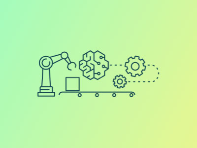
Running EDA and related workloads in the cloud allows chip designers and verification engineers to solve complex, compute-intensive problems, enabling you to reduce time-to-results by scaling to larger numbers of parallel tasks than would be practical in most on-premises environments.
-
Securely store, categorize, and analyze all your production data in one, centralized repository. Add a wide variety of cost effective and powerful analytics products to process, analyze, and visualize data.
-
Focus on improving business operations, and innovation, not IT and OT infrastructure. AWS pay-as-you-go, microservices, and serverless computing models reduce the cost of running connected plant or product implementations. With minimum upfront investments and nearly unlimited on-demand capacity, you can focus on differentiating your business not on infrastructure.
-
Cloud security at AWS is the highest priority. As an AWS customer, you benefit from a data center and network architecture built to meet the requirements of the most security-sensitive organizations.
Semiconductor and Hi-Tech Electronic Customer Stories
We work with the industry's leading semiconductor and hi-tech electronic companies who expect more from their technology partners and know that experiences speak louder than words. Learn more about the exciting ways these companies are leading their cloud journey with AWS.
AWS transforms semiconductor and hi-tech electronic operations with cloud technology
Industry customers use AWS to innovate faster, optimize performance, improve interoperability with partners and customers, and grow revenue across four solution areas aligning to their highest-priority use cases: Design & Verification, Supply Chain, Sustainability and Manufacturing Intelligence.
Solution areas
Interested in AWS for Industrial?
If you are an asset-intensive industry like manufacturing, energy, mining, agriculture, transportation and utilities, it’s time to discover how AWS for Industrial can help you get the most out of your data.

Innovate with key industry partners
Discover semiconductor solutions and services from an extensive network of industry-leading AWS Partners who have demonstrated technical expertise and customer success in building solutions on AWS.
See all AWS Industrial Software Competency Partners »
Featured partners
AMD
Synopsys
Cadence
Siemens
 Siemens EDA, a segment of Siemens Digital Industries Software, is a technology leader in software and hardware for electronic design automation (EDA). Siemens EDA offers proven software tools and industry-leading technology to address the challenges of design and system level scaling, delivering more predictable outcomes when transitioning to the next technology node.
Ansys
Amazon FSx

Ready to start your industrial transformation?
Leading manufacturing companies are already using AWS. Contact our experts and start your own AWS journey today.
Get Started with AWS