Solutions for Hi-Tech Electronics and Semiconductor
Discover curated Solutions that address varied hi-tech electronics and semiconductor use cases
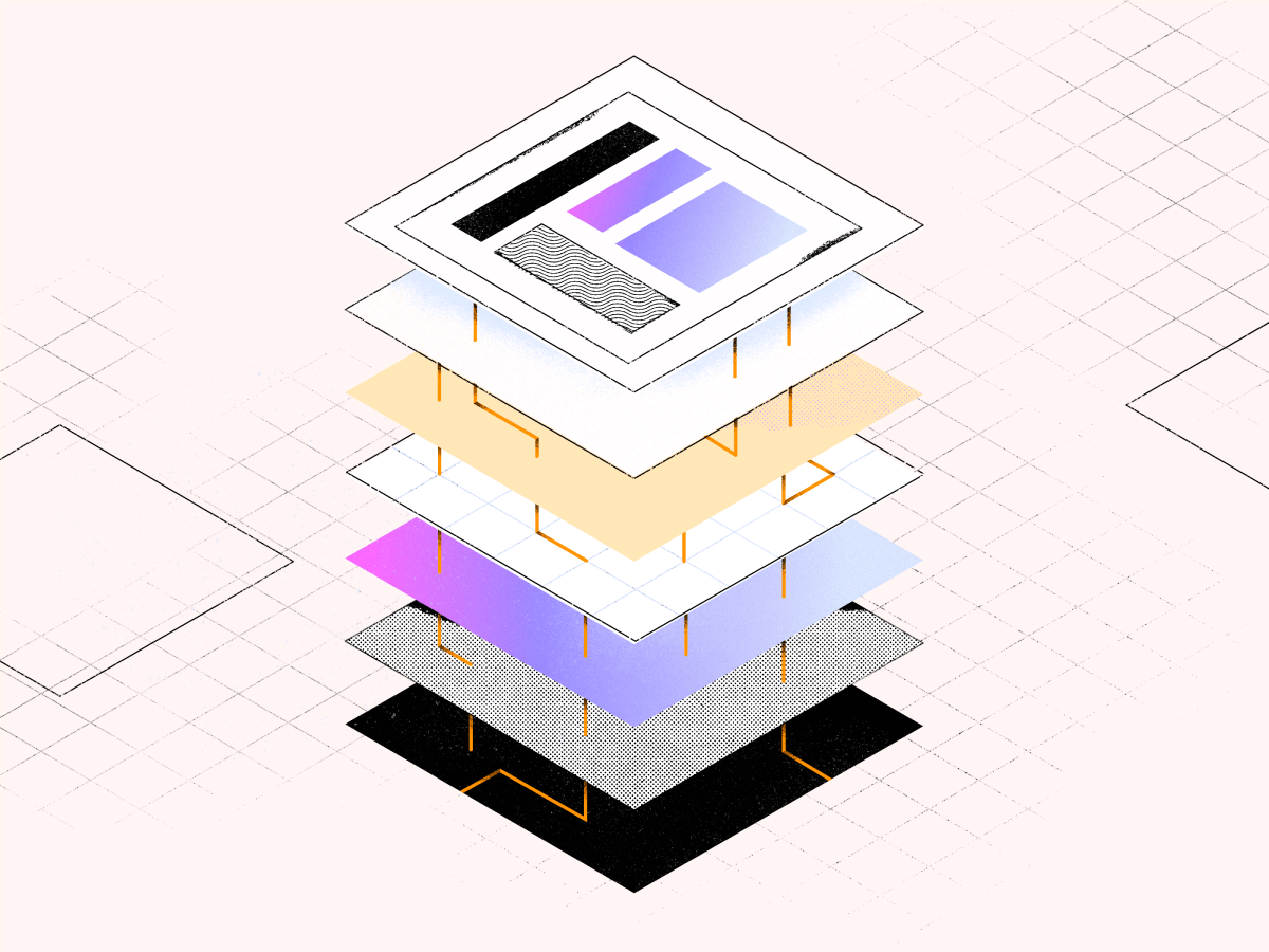
Transforming hi-tech electronics and semiconductor with AWS
Hi-Tech Electronics and Semiconductor Solutions on AWS accelerate electronic design automation, optimize yield management, and scale new product development and introduction. Unlock the full potential of the cloud and innovate faster. AWS offers the broadest set of services, Solutions, and Guidance coupled with AWS industry Partner Solutions to make it easier to select the right tools for your highest-priority workloads.
Browse Solutions for hi-tech electronics and semiconductor
Explore AWS Services, ready-to-deploy AWS Solutions, specialized Partner Solutions, and architectural Guidance for your hi-tech electronics and semiconductor use cases.
Loading
Loading
Loading
Loading
Loading
Did you find what you were looking for today?
Let us know so we can improve the quality of the content on our pages