AWS for Industries
Siemens PCBflow – Design validation for first-time-right manufacturing
Introduction
First-time-right design is critical to cutting costs and reducing time to market, especially in today’s customized, high-demand environment. If you’re a Printed Circuit Board (PCB) designer or involved in PCB manufacturing, keep reading to learn more about Siemens PCBflow.
PCBflow is a new cloud offering in the PCB Design for Manufacturing (DFM) domain, can give you the first-time-right design advantage. This post covers the challenges of current validation processes, explains how the new technology overcomes those challenges and details the architecture and tools behind the new innovative solution.
The Printed Circuit Board industry and Siemens PCBflow
In recent decades, many industries have witnessed an acceleration in both the design and the manufacturing processes of their core business. On one hand, the design process has become more agile as new collaborative tools have appeared on the market and various design patterns and standards have emerged. Manufacturing, on the other hand, has gained velocity due to lower prototyping costs, automation, availability of skilled labor and other industry-specific factors.
The acceleration in the design and manufacturing processes has made it more crucial than ever to achieve first-time-right design.
Reducing the number of iterations between the designers and manufacturers (sometimes referred as “implementers”), allows companies to cut costs and significantly reduce time to market, thus gaining a competitive advantage.
The Printed Circuit Board (PCB) industry is not exceptional, and design validation tools are crucial in order to meet the high demand while maintaining low costs. Siemens PCBflow is a new cloud offering in the PCB Design for Manufacturing (DFM) domain that gives customers the first-time-right design advantage.
Design done right
Design validation for implementation is a common challenge that affects profit margins. The old saying holds true: “It costs a penny to make a change in engineering, a dime in production and a dollar after a product is in the field.” To save these dollars and dimes many innovative tools have emerged on the market. Despite the different problem domains, most of them share common traits, including PCB DFM.
Adhering to design rules
The validation process usually consists of one or more phases each corresponding to a different element that requires testing. In every phase, the design undergoes evaluation against a specific set of rules. The process is facilitated by a rule engine service that evaluates the rules from a dedicated rule library. In many domains, the rules are primarily data-driven and depend on different attributes of parts (physical or other) used in the design.
The resources required in this process vary. The complexity of the design validation depends on the algorithms used, as well as on the diversity of components and the dependencies between them. Validation tools were historically developed as desktop applications for designers, allowing them to create or view the design as well as to assess its validity. Using these tools for large, complex designs required significant computing resources.
Another challenge facing validation tools is the availability of up-to-date data, such as rules and component catalogs. A small local database is commonly used as a storage solution due to the sheer size and complexity of these libraries.
To satisfy the above, validation tools are often installed on high-end desktop computers, adding to the end customer’s total cost of ownership. Buying an on-premises validation tool means extending capex on suitable hardware. Even with a cancelable license, the customer has to absorb the sunken costs of the workstations. While this could be an acceptable risk for an enterprise, it can be a barrier for smaller businesses interested in purchasing such a solution.
Keeping up-to-date design rules
In order to keep up with the market demands, vendors update their catalogs – new components are added and others are retired. New knowledge is accumulated and new catalogs and rules are created to validate designs. These changes require daily or weekly updates of the validation tools in multi-vendor part catalogs.
Creating and distributing such frequent updates to the install base creates operational overhead that doesn’t scale well. Discrepancies between versions of the validation software, catalogs and rule libraries cause the design versions to be valid only against certain versions of the catalog. This presents a significant barrier to collaboration between different technical professionals involved in the validation process. Streamlining the validation workflow is key to efficient design operation but, as we’ve seen, it is not easy to achieve.
So, is there a better way?
Siemens PCBflow – Accelerating electronics manufacturing with a SaaS solution
Printed Circuit Boards (PCBs) are the base of many products today, from wristwatches, to smart TVs, washing machines, fighter jets and satellites. PCBs consist of numerous electronic components and layers of copper wiring. While designing a PCB is a complex process, confirming that the design can actually be manufactured is even more challenging. The PCB designer needs to address the PCB’s specific electronic requirements while ensuring that the PCB can be manufactured and tested.

In the highly competitive electronics industry, time to market is a key factor in business success. Vendors can no longer afford to waste time on numerous, expensive iterations between the PCB designers and manufacturers.
Siemens ValorNPI: Analytics Tool as a Service
To date, Siemens Valor NPI analytics tool, a globally renowned tool for DFM validation of PCB designs, was only offered as an on-premises, single-tenant solution. Therefore, it was accessible only to larger companies, due to the infrastructure investment and maintenance overhead.
With PCBflow, the novel Software-as-a-Service (SaaS) solution for PCB DFM validation, Siemens has expanded its product accessibility to new market segments including startups, mid-sized manufacturers and design houses.
As a SaaS solution, PCBflow has enhanced the DFM analytic service with the capability to provide efficient, real-time collaboration between everyone involved in the design and product manufacturing. Its ability to securely handle data in the cloud makes PCBflow a trusted hub for designers and manufacturers to share designs and validate them against the manufacturer’s specific constraints. A unique, patent-pending mechanism was designed and implemented to ensure the privacy of any shared data.
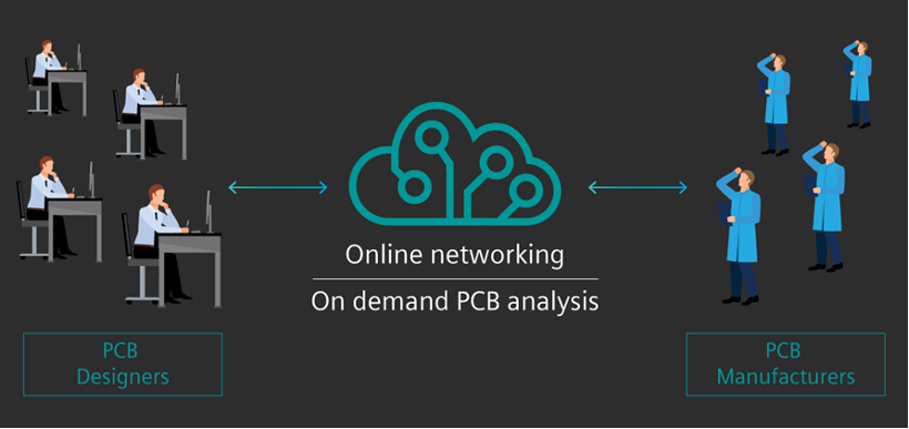
The managed solution offers a streamlined process and reduces the need for hardware, maintenance or data requirements in order to synchronize part catalogs or rule libraries. The flow is simple: designers upload the PCB design, while manufacturers upload their constraints. This makes it possible to run a DFM analysis specific to a certain manufacturer and thus reduces time to the final product. The entire process is secured and managed entirely by Siemens’ cloud services.
The architecture and tools behind the solution
Built on AWS, PCBflow provides its users the necessary level of security to be a trusted hub for designers and manufacturers. AWS Identity and Access Management (AWS IAM) allows Siemens to control access on the lowest level of the solution’s cloud resources. Each PCBflow service carries a unique role with limited permissions, limiting its access to the resources it needs. Design and manufacturing constraint documents are securely stored in Siemens’ cloud storage solution leveraging the Amazon Simple Storage Service (Amazon S3) and are encrypted at rest with keys managed by AWS Key Management Service (AWS KMS). Session data is securely stored in Amazon DynamoDB, a highly scalable, low-latency NoSQL document database.
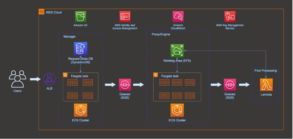
The computing resources for the design validation process are provided by the Amazon Elastic Container Service (Amazon ECS), allowing it to run containerized workloads with the ability to meet the demand at any moment, scaling out and in according to need, with low management overhead. The solution’s logging and event monitoring are based on Amazon CloudWatch, utilizing its ability to provide insights on the system’s performance and alerts and notifications as needed.
To address the challenges of long design to manufacturing cycles, affecting the profit margins in the PCB manufacturing industry, AWS and Siemens has partnered to deliver a scalable SaaS solution – Siemens PCBflow. Powered by the AWS services under the hood, this solution is offering a simple and a secure way for PCB designers and manufacturers to collaborate – building a better future for all of us.
Learn more
For more information on PCB Design for Manufacturing validation solutions in the electronics industry, visit Siemens PCBflow and PCBflow Blog, as well as PCBflow on-demand webinar.
If you’re interested in learning more about how AWS can help grow your Manufacturing or Industrial business, please visit AWS for Industrial.
For additional insights on AWS services, powering PCBflow, please visit Amazon ECS, Amazon DynamoDB and Amazon S3.