AWS for Industries
How NXP is Moving Chip Design to AWS
In 2021, NXP selected AWS as its preferred cloud partner to migrate the vast majority of its silicon design workloads from NXP data centers to AWS. The migration is well underway, and a number of teams have already taped out projects in their AWS cloud environment. In this blog post, we share more about NXP’s cloud journey: the rationale to move, the early architecture decisions, and a few lessons learned along the way for migrating silicon design workloads to AWS at enterprise scale.
Why move silicon design to AWS, and why now?
With a diverse product portfolio, NXP’s design engineers design and verify a wide range of chips, across multiple design centers around the world. The most common workloads are library characterization, DFT, layout, place & route, and circuit simulation. For years, NXP has taken advantage of the flexibility of AWS by leveraging the elasticity of the cloud when demand for on-premises EDA infrastructure spiked. The company would burst peak demand into AWS when the static on-premises computing environments reached full utilization. But as chip projects moved towards more complex advanced-node designs and new mission-critical use cases, infrastructure needs continued to increase non-linearly, and it became more challenging to manage the widening gap between the peaks and valleys of demand. Continuing to invest on-premises would have meant continuing with multi-year commitments to the same pieces of hardware. Doing that while the industry experiences such dynamism, fluctuation, and need for agility would have been a risky and capital-intensive endeavor.
Meanwhile, NXP observed the acceleration of innovation and cost reductions occurring in AWS. New specialized Amazon EC2 instance types for high performance computing were being unveiled at a rapid clip, and the broadening range of Intel, AMD, and AWS Graviton-based instances would allow NXP to experiment and meet the unique requirements of each design project while achieving a higher level of performance at reduced overall costs. With the acceleration of these trends, NXP decided the time was right to bring end-to-end silicon design workflows to the cloud, giving its silicon engineering teams the best available infrastructure for designing the company’s next-generation chips. The only question was how: will NXP be able to run end-to-end design workflows on AWS in a cost-effective way and provide a non-disruptive path to migrate the entire design community?
Taking the leap
Evacuating the vast majority of NXP data centers and migrating over 8,000 design engineers to a new cloud-based design platform is not a decision taken lightly. Through comprehensive PoCs and pilot programs, NXP evaluated various cloud providers to understand performance, costs, and functional feasibility. These extensive evaluations had to prove that an end-to-end design flow could run on cloud compute and storage infrastructure with better price performance than on-premises. It also needed to show that a move to the cloud would not be overly disruptive to the already busy engineering support organizations, and surely not for the end users.
Within the last decade, NXP executed a plan to standardize and consolidate the engineering IT infrastructure and create a common design environment to serve its globally distributed design community. This standard, known as the NxDI Design Platform, provides a blueprint for a consistent and predictable user experience regardless of the type of project or where it is executed. NXP engineers depend on the global consistency enabled by NxDI, and preserving the on-premises user experience became a key business requirement that would inform the cloud architecture. The look and feel of the cloud design environment should be familiar to the engineering teams, and it should be functionally equivalent. Guided by this design principle, NXP worked closely with solutions architects and semiconductor industry specialists from AWS to design a cloud architecture and a plan for migration.

Figure 1: NXP’s NxDI Design Platform on AWS
Similar to their standard on-premises engineering IT infrastructure architecture, NXP’s silicon design environments on AWS comprises four primary service layers: an elastic cluster of high-performance compute servers, scalable file storage, shared services, and virtual desktops that serve as an interactive entry point for engineers. Each component in these layers has a unique purpose and is managed by a specialized IT service team. The components were divided into their own AWS accounts to align with the company’s IT support structure and operating model. A shared VPC ensures direct network communication between the components, and security groups, authentication, and encryption are used to secure the environment at multiple levels. Separate environments are created for each engineering project. Isolating projects in this way improves security, minimizes the “blast radius” of operational events, and makes it easier to perform cost allocation across finance domains. A set of common services is shared between the project environments.
Amazon CloudWatch is used to collect OS- and application-level metrics. CloudWatch Logs collects log files from the environment and metric filters convert the log data into actionable metrics. NXP relies on AWS Direct Connect to provide high bandwidth, low latency access to and from their existing on-premises environment.
Design data management (DDM) software provides revision control and distribution of tech and IP libraries and other design data. The primary design data management server lives in AWS and mirrors data back to the on-premises environment.
A central tools repository holds the EDA tools required by the project teams. Today, the repository is replicated into AWS using rsync. Plans are being made to transition this process to AWS DataSync in the near future.
These infrastructure layers and peripheral services are combined to provide an elastic computing environment that matches the right resources to the workloads and expands and contracts based on demand, enabling engineering teams to reduce design cycle times in a familiar environment while only paying for what they use.
Choosing the storage
When NXP started on AWS, Amazon FSx for Lustre was the logical shared storage solution for its fast, scale-out throughput performance, which is well suited for HPC workloads like silicon design. With FSx for Lustre, NXP can deploy fully managed file systems in minutes, reducing the onboarding time for new projects.
NXP began evaluating Amazon FSx for OpenZFS and Amazon FSx for NetApp ONTAP shortly after they were announced in late 2021. Both fully managed high-performance file systems are accessible through NFS and support volume level snapshots, a storage feature that is important to NXP. With snapshots, users can easily view and restore individual files or folders from an earlier point in time. They do this in a self-service manner by browsing .snapshot (ONTAP) or .zfs/snapshot (OpenZFS) directly from their VDI desktop, further reducing administrative workload for storage administrators. This makes it an excellent fit for home or project directories where quick file-level restores are frequently needed.
FSx for NetApp ONTAP also provides familiar NetApp features such as SnapMirror and FlexCache, which can accelerate regional expansions or data migration to AWS without changing NXP’s administrative workflows. Early benchmark results show performance improvements of up to 2x (read) and up to 3x (write) over their on-premises storage solution.
FSx for OpenZFS also provides low-latency (a few hundred microseconds), high-performance shared file storage. NXP’s initial tests show that FSx for OpenZFS provides up to 7x better throughput and IOPS performance for frequently accessed data served from cache compared to their on-premises file servers. Exporting an FSx for OpenZFS volume using the async option provides further improvements in write performance by enabling the file server to acknowledge client I/O requests as complete when they are written to the file system’s in-memory cache rather than when they are committed to the server’s disks. This is a useful configuration for scratch file systems.
Testing is ongoing, but it is likely that NXP will optimize for price and performance by matching the file system’s feature sets, performance profiles, and data management capabilities to the needs of their workloads. For example, small-file and heavy metadata workloads could land on FSx for NetApp ONTAP and FSx for OpenZFS because of their strong small-file performance and like-for-like replacement with existing on-premises environments, while FSx for Lustre continues to serve back-end workloads that benefit from hundreds of GBs/s of throughput.
Choosing the correct compute
NXP conducted workload throughput performance tests using a variety of Amazon EC2 instances that are well suited for silicon design workloads. Z1d and M5zn instances provided the highest performance because of their high all-core turbo CPU clock speeds. But at the time, NXP determined that C5 instances offered the best price performance for a majority of their workloads and use cases. For simulations that required a larger memory footprint, M5 proved to be the sweet spot.
NXP is now moving workloads towards the recently released M6i and C6i instances. Early tests show ~20% improvement in price performance for their design workloads. Refreshing their compute environments with the latest generation CPUs, like the Intel “Ice Lake” processors found in the M6i and C6i, can be completed in a few hours and gives NXP an immediate price performance benefit. These types of compute refreshes took months to achieve in the company’s on-premises environments. With the goal of improving price performance even further for some key workloads, NXP has plans to test EC2 instances based on the AWS Graviton2 ARM-based server processor. With several commercial EDA tools now available for ARM-based processors, NXP hopes to continue to drive down costs of verification and library characterization workloads with Graviton2-based instances.

Figure 2: Benchmark results comparing various on-premises compute servers and EC2 instances.
Early production results
Today, NXP has completed multiple tape-outs on AWS and has all major design teams running their projects in the cloud. These teams run their design flows independently in the cloud, with the exception of EDA license infrastructure, which is planned to be migrated to cloud in 2022. Data storage has surpassed 2.5 petabytes and over 100 million core-hours have been consumed.
What NXP likes most about its new cloud-based design environment is the agility that it provides. Although the new environment feels familiar to the users, project teams experience a much quicker cycle time because of the elastic nature of the infrastructure. Compute capacity grows and shrinks as needed to match demand. Additionally, engineering teams appreciate being able to dynamically tune the mix of instance types to accommodate the changing requirements of their workloads. Together, these capabilities provide a level of flexibility, performance, and efficiency that was simply not possible on-premises.
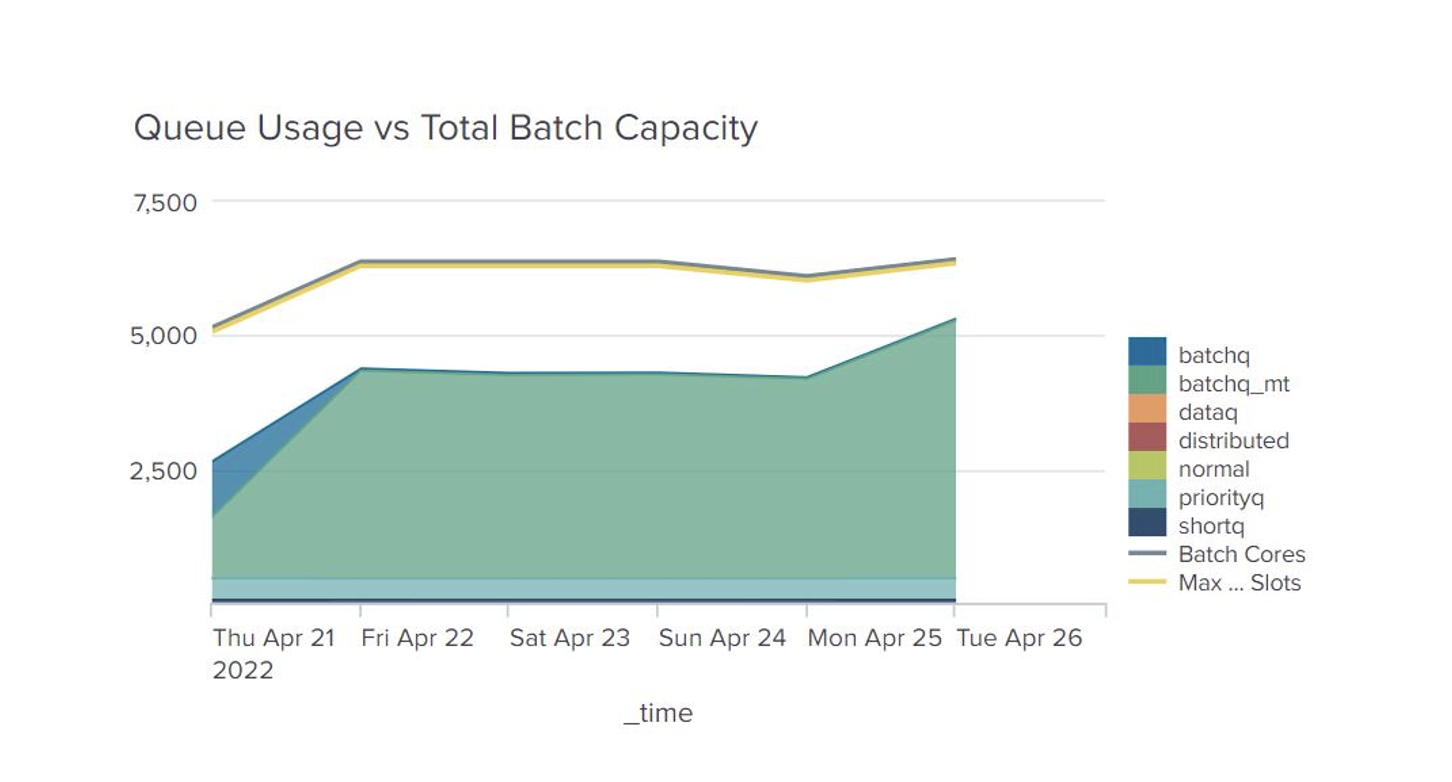
Figure 3: Dynamic compute scaling at work in one of NXP’s AWS-based silicon design environments. The y-axis represents the number of job slots, or CPU cores, in the computing environment.
Lessons so far and roadmap
There is no single playbook for moving silicon design to the cloud, as organization structure, ways of working, and culture vary between semiconductor companies. Like NXP, organizations planning to migrate to AWS often chart their own way, partnering with AWS semiconductor industry specialists and solutions architects to devise an architecture and migration plan that best suit their business needs. Looking back at their experience, NXP noted key decisions that were crucial to the success of their cloud journey:
- Within NXP, like in many semiconductor companies, there is a clear delineation between engineering, CAD management, IT management, and the finance and procurement teams that support their data center expansion and refresh needs. An important part of NXP’s cloud migration strategy was to bridge these groups together through executive-level sponsorship, including establishing the business drivers (reducing schedule risks, enabling M&A activities and external collaboration, increasing the ability to launch new products with shorter lead times, etc.) that motivate a move to cloud. For example, the NXP CIO played a key role in aligning senior leadership and setting goals with C-level mandate. Without such leadership, the effort could be easily blocked by individual teams and the business case diluted. Top-down goals signal to the organization that it is a priority to make this transformation. This forces teams to move faster than they would organically.
- The leading design principle of maintaining the look and feel of the on-premises end-user experience proved to be an advantage to get the first teams to move to the cloud. This enabled these chip projects to ramp up quickly and leverage the benefits of AWS. NXP found that most existing toolsets, processes, and flows could be shifted to the cloud, and the AWS platform could be tuned to their needs.
- A comprehensive change plan covering all angles, such as architecture, automation, business case, business unit adoption, support organization, and operating model, was key. The stakeholders agreed it was important to have a plan that could be monitored with agreed upon KPIs.
- Cloud migrations are done by great teams with cloud skills, and enabling NXP’s existing staff with the right cloud skills ahead of the migration was critical. Over 100 team members from NXP’s engineering IT and other support organizations went through an intensive learning program that included AWS immersion days, AWS training classes, and technical deep-dive sessions on specific topics. These enablement programs were a crucial part of the journey. In addition, NXP found that a PoC with their own workloads was one of the best ways to learn the ins and outs of tuning AWS services to fit their needs.
Looking forward, the company is planning to provide even more capabilities to their engineering teams with the cloud. The NXP IT team now realizes they have much more flexibility to chart their own path and will use AWS services when it makes sense to support the design community. For example, because they automate many of the infrastructure deployments using infrastructure-as-code with AWS CloudFormation, they can create a quick and repeatable process to deploy secure collaboration chambers in the AWS Cloud on an as-needed basis. This will enable the businesses to deploy isolated environments for collaborative design projects or debug sessions with 3rd parties faster, with much less effort from IT. Similarly, NXP has developed a full roadmap of continuous improvement and optimization, including plans to adopt more native AWS services and features such as Amazon SageMaker, a fully managed machine learning service, to forecast project usage of cloud resources and optimize costs and performance with intelligent job scheduling and resource management.
To learn more about silicon design on the AWS Cloud and how other semiconductor companies are benefitting from the scale and performance of AWS infrastructure, visit the AWS Semiconductor and Electronics page.