AWS for Industries
The semantics of data sharing across the semiconductor supply chain
Introduction
As the global supply chain continues to impact the semiconductor industry, it is vital to find a better way to forecast demand and predict supply chain shortfalls. As a follow-on to my interview and content provided in Architecture Monthly: Semiconductor Design, this blog discusses the need for cross-industry data sharing and collaboration, and the benefits to running your design, verification, manufacturing, and test workflows on AWS. A critical component is the ability to share data both upstream and downstream. To illustrate this, we’ll look at the cyclic nature of the semiconductor supply chain as it currently exists today, and building on that to improve chip design, reduce costs, and improve time to market.
Running on AWS
It is well known across the industry, that you can run your workflows on AWS in nearly the same way that you are running them today in on premises data centers. Amazon Elastic Compute Cloud (Amazon EC2) offers the fastest processors in the cloud and we are the only cloud with 400 Gbps ethernet networking. Additionally, with our recent storage announcement, Amazon FSx for NetApp ONTAP, customers have the option of using a familiar storage platform that supports hybrid workflows between AWS and on premises. Now that customers have seen the benefits that AWS can provide for semiconductor workflows, we are now seeing collaboration, data sharing, and business insights where it didn’t exist before.
The semiconductor supply chain
In Figure 1 below, I created a diagram that shows the semiconductor supply chain. This diagram illustrates the high-level dependencies that exist across the industry. The initial process starts with the customer’s specification, and that is given to the semiconductor design house or an IDM (Integrated Device Manufacturer). From there, all the familiar steps follow that lead to tape-out and delivering a product to the field.
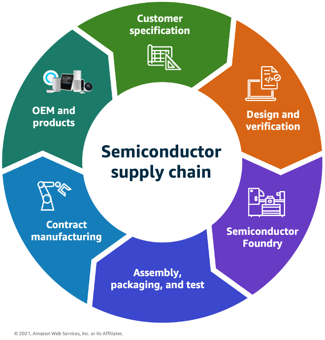
Figure 1: Semiconductor supply chain
In Figure 2 below, I have added the input and output for each step, and this shows the flow and cyclic process of taking a chip to market. This is the traditional direction, and although this unidirectional process is still an integral part of the supply chain, the vital next step is enabling cross-industry data sharing.
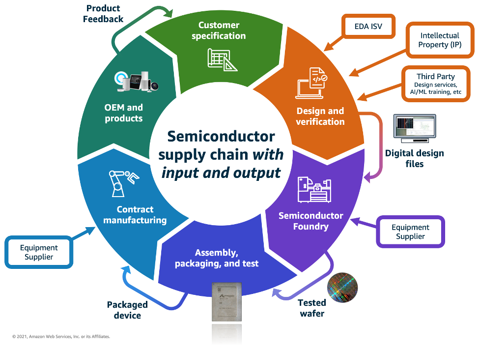
Figure 2: Semiconductor supply chain with input and output from each step
Pervasive collaboration
What Figure 2 does not show is the on-going and pervasive need for collaboration across the entire industry. Examples include, third party design, OSAT, and working with your fabrication facility. Often chip design companies will not have the in-house resources to design and verify an entire chip, relying on third parties to do, for example, physical design. Collaboration between the foundry and OSAT company is needed to update equipment (software/firmware patching) and enable predictive maintenance using sensor technologies coupled with AI/ML. Another example is data sharing between the foundry and design company to help with wafer yield analysis. Expanding on this in Figure 3 below, is a high-level architecture diagram that shows data flow between the on-premises data center, foundry, and the fabless semiconductor company’s AWS account. Specifically, data sharing is enabled with the use of a secure collaboration chamber, which is an Amazon Virtual Private Cloud (Amazon VPC) with the security and network configurations required for semiconductor workflows. In a future blog post, we will detail the process of setting up and configuring secure collaboration chambers.

Figure 3: Secure collaboration enabled with Amazon VPC
In Figure 3 above, we see the same steps in the semiconductor supply chain as the previous diagrams, but here I have broken this down to show specific data movement. I’m showing how the foundry and semiconductor design company can easily share data by using a secure collaboration chamber. This secure collaboration chamber (aka Collaboration VPC) that is being used for wafer yield analysis is owned and controlled by the fabless semiconductor company, but allows for foundry and on-premises data center access. Additional detail and specific services used can be found in the official Reference Architecture diagram I authored: Semiconductor and Electronics on AWS, and in the upcoming blog post on collaboration chambers.
Solving supply chain issues
Now that we have discussed traditional architectures and how AWS is extending those to enable collaboration and data flow across the industry, let’s focus on the big picture and addressing global supply chain issues. AWS provides a globally accessible cloud platform that allows customers to move data, and more importantly, access that data, in a region that is geographically beneficial. This is a straightforward process of ensuring that you are using the correct AWS Region (work with your AWS Solutions Architect or Partner to facilitate this process). We continue to see an increase in customers using AWS for semiconductor workflows, but now we are seeing customers struggling to find common semantics that enables data sharing across the entire industry, while giving at least the option, if not the standard, for anonymity. That is, although some information is being shared across the industry, for example from foundries to design houses, what we are not seeing is a globally, concerted effort to define an industry standard for data sharing and preservation of anonymity. Although this may not be a short term solution to the supply chain issues, working with you, the semiconductor community, this is what we are working to figure out. In Figure 4 below, the direction for data sharing should be, at a minimum, the reverse path of chip design, and ideally data sharing should be an inter-connected collaborative effort that allows customers to securely and anonymously move data across the entire supply chain.
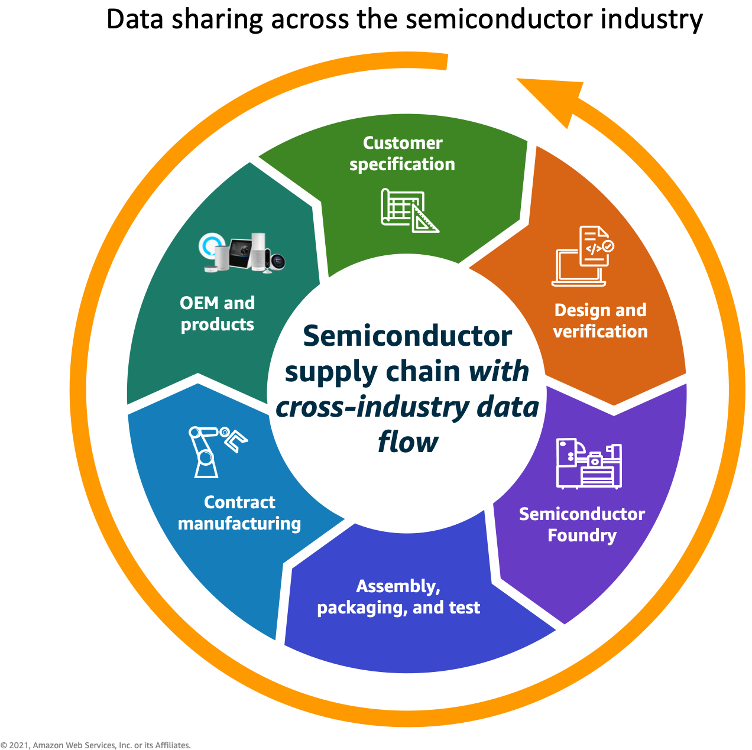
Figure 4: Data sharing across the semiconductor industry
Summary
We understand that there are legacy systems, that data may require translation, and there are decades old manual processes that need automation. At AWS, we have the tools and working with you, we can build the solutions to enable truly cross-industry collaboration and data sharing. But first, we as an industry, need to figure what language (semantics) to use.
We are at DAC next week in booth #1252 , please come by to chat with us and share your thoughts.
For more information about running your workflows on AWS: AWS Semiconductor and Electronics Resources