AWS for Industries
Solution for Open-Source Chip Design on AWS
In this blog, we discuss the benefits of using open-source electronic design automation (EDA) software, which is required for designing integrated circuits. We also discuss why AWS is the best platform to do open-source chip design and an effective means to collaborate and enable academia and chip design teams with a lower budget to design their own chips.
Why we need Open-Source Chip Design:
According to the Semiconductor Industry Association (SIA), there are over 277,000 workers in high-paying R&D, design and manufacturing jobs across 49 states. Deloitte predicts that more than one million additional skilled workers will be needed by 2030, equating to more than 100,000 annually. Today, hardware design & research at academia and startups is hindered by the combination of factors such as the need for proprietary tools, the shortage of expert users who can use these tools in advanced technologies, and the significant cost and risk associated with attempting hardware design. These factors have created obstacles in the way of meeting the demand for additional semiconductor workers.
Furthermore, chip design software is faced significant challenges, such as the need to deal with vast amounts of data and ever-increasing design complexities, ensure design accuracy and integrity, and provide fast and efficient design verification and validation. As shown in Figure 1, the semiconductor industry has struggled to keep product design costs under control, despite the advancements in hardware design tools and methodologies. The US government recently stepped in and announced CHIPS for America Act that plans to invest $280 billion to bolster US semiconductor capacity, catalyze R&D and create regional high-tech hubs and a bigger, more inclusive STEM workforce.

Open-source software development helps solve several aforementioned challenges and has significant benefits for software development as a whole. Some of the key advantages include lower cost of development, fostering innovation, ease of access, improved software quality and interoperability with a wide range of platforms and systems.
Introduction to Open-Source EDA
Open-source Electronic Design Automation (EDA) is a rapidly growing movement within semiconductor academia and industry. By leveraging the power of collaboration and open-source software, open-source EDA provides researchers, students and other academics with access to cutting-edge tools, methodologies, and technologies that were previously only available to large scale semiconductor firms. This movement is driven by a growing desire to reduce the barriers to entry in hardware design, increase collaboration and knowledge-sharing within the industry, and provide more affordable and accessible solutions for engineers, researchers, and academics.
“Designing a chip in your garage should be as easy as designing a mobile app in your garage” – Tom Spyrou, Chief Architect of OpenROAD
In June 2018, with the help of funding from DARPA MTO’s Intelligent Design of Electronic Assets (IDEA) program, OpenROAD was funded. OpenROAD is an open source, no-human-in-loop, 24-hour chip layout design solution for Application Specific Integrated Circuit (ASIC) and System on Chip (SoC) design teams, the solution aims to reduce the barriers of cost, expertise, and unpredictability that currently hinder innovation in the semiconductor industry, which are often present in proprietary solutions. OpenROAD has already been used in over 600 tapeouts and has been successful on process nodes down to 12nm. Due to its ease-of-use, an increasing number of companies are starting to use OpenROAD early on in the development process, during hardware and software architectural exploration, which is particularly useful when testing new architectures and algorithms where empirical power, performance, and area (PPA) data is not available.
“Seeding the future – Linux of EDA” — OpenROAD Project
OpenROAD supports mature nodes & open source PDKs from Global Foundries and Skywater such as GF180 (180nm) and Skywater130 (130nm) and advanced node proprietary PDKs from TSMC, Global Foundries and Intel Foundry Services such as TSMC65 (65nm), GF12 (12nm), Intel22 (22nm) and Intel16 (16nm). The ASAP 7nm Predictive PDK developed by Arizona State University in collaboration with ARM Research is also supported by OpenROAD and enables the academic community to research, prototype and develop advanced 7nm finFET based designs.
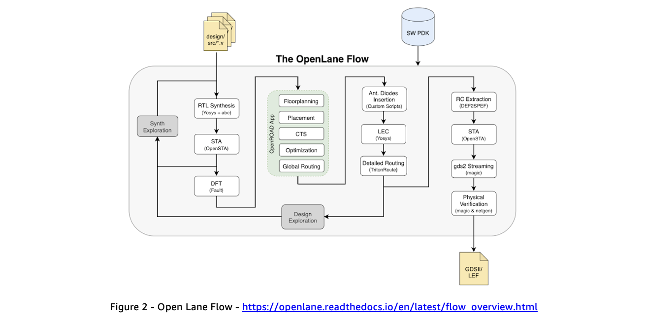
As a project of the broader open source EDA Initiative, OpenLane, developed by Efabless, is an open source automated RTL to GDSII flow based on several components including OpenROAD and other open source EDA software tools such as Yosys, Magic, Netgen, CVC, SPEF-Extractor, KLayout and a number of custom scripts for design exploration and optimization. It also provides a number of custom scripts for design exploration, optimization and ECO. Figure 2 shows the architecture of the OpenLane flow.
nClouds, an AWS partner, providing DevOps consulting and implementation services has partnered with Efabless to modernize its integrated circuit (IC) design platform to improve performance efficiency and scalability, enhance security, and optimize costs. OpenLane is also now being used by several universities including University of California, Berkeley, University of California, San Diego, and the University of Costa Rica.
Open-Source EDA on AWS
Open-source EDA enables researchers to leverage modern computing systems powered by the cloud to deploy EDA at scale. As an example, the OpenROAD project, AutoTuner, allows designers to automatically set up and execute thousands of experiments on the cloud thereby achieving PPA possible at a fraction of the cost and 3X faster runtime. The results were achieved via a Kubernetes cluster with a provision for distributed detailed routing with one load balancer and 30 servers of 15 CPUs. Detailed testing on the router provided clear insights into architectural tradeoffs of distributed vs multi-threaded processing, single vs multiple machine configurations. The OpenLane RTL-to-GDSII flow was developed to be run as a docker container which enables flexibility in running it in the cloud, enables scalability, minimizes the dependency on an exact Linux Configuration and reduces administrative overhead and costs. In the subsequent sections, we will demonstrate how designers can get started with their open-source EDA on AWS.
How to start designing your open-source chip on AWS:
To help you get started with building your open-source EDA project, we will outline several AWS services that can be utilized. EDA workloads often require a compute cluster, a process scheduler that orchestrates job distribution to compute nodes, and a high-performance shared file system. The shared file system, typically required to sustain throughput requirements for an EDA workload can vary anywhere from 500 MB/sec to 10 GB/sec depending on the EDA workload use case, design size, and total number of cores. For quickest and simplest start, start by setting up a NICE DCV based remote visualization on an EC2 instance. We will then go over a sample reference architecture that has several key components necessary to run open-source EDA workloads such as Remote Desktop Visualization, Elastic Storage, Scalable Compute cluster and Job Management system all with a highly secure posture.
NICE DCV Visualization EC2
NICE DCV is a high-performance remote display protocol that provides customers with a secure way to deliver remote desktops and application streaming from any cloud or data center to any device, over varying network conditions. The NICE DCV AMI for Amazon Linux 2 is available on AWS Marketplace for free. For running EDA workloads, NICE DCV allows designers to easily visualize EDA CAD applications on Linux based desktops. NICE DCV features:
To get started with NICE DCV, simply do the following:
Deploy:
- Create and activate your AWS account.
- Sign in to your AWS Management Console.
- Select the appropriate NICE DCV AMI from the AWS Marketplace or download and install the appropriate NICE DCV server on your EC2 instance and generate an AMI with your application stack.
- Deploy EC2 instances with NICE DCV server installed after making sure your security group inbound rules allow traffic on port 8443.
Connect:
- Download and install the appropriate NICE DCV native client on your device.
- Connect to your remote machine with the NICE DCV native client or web client using https://:8443.
Stream:
- Clone the OpenLane git repository and follow instructions to run the OpenLane flow.
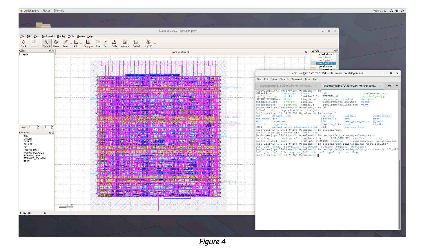
- Stream your graphics applications across devices using NICE DCV. (Figure 4)
- For more detailed information, refer to this link.
Shown below is a screenshot with a KLayout visualization of a GDS file of a final test design layout after running OpenLane using the sky130 technology PDK. The OpenLane test flow was run m5.2x.large EC2 instance on Amazon Linux 2 with a NICE DCV based Amazon Machine Image (AMI).
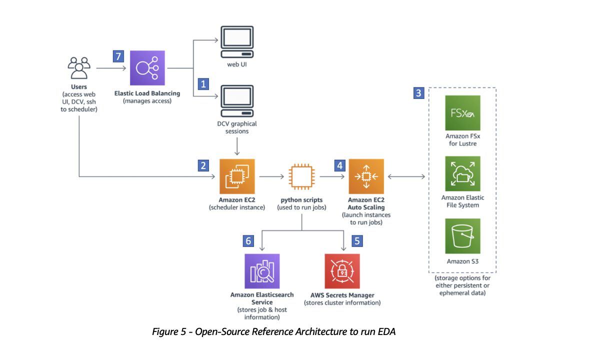
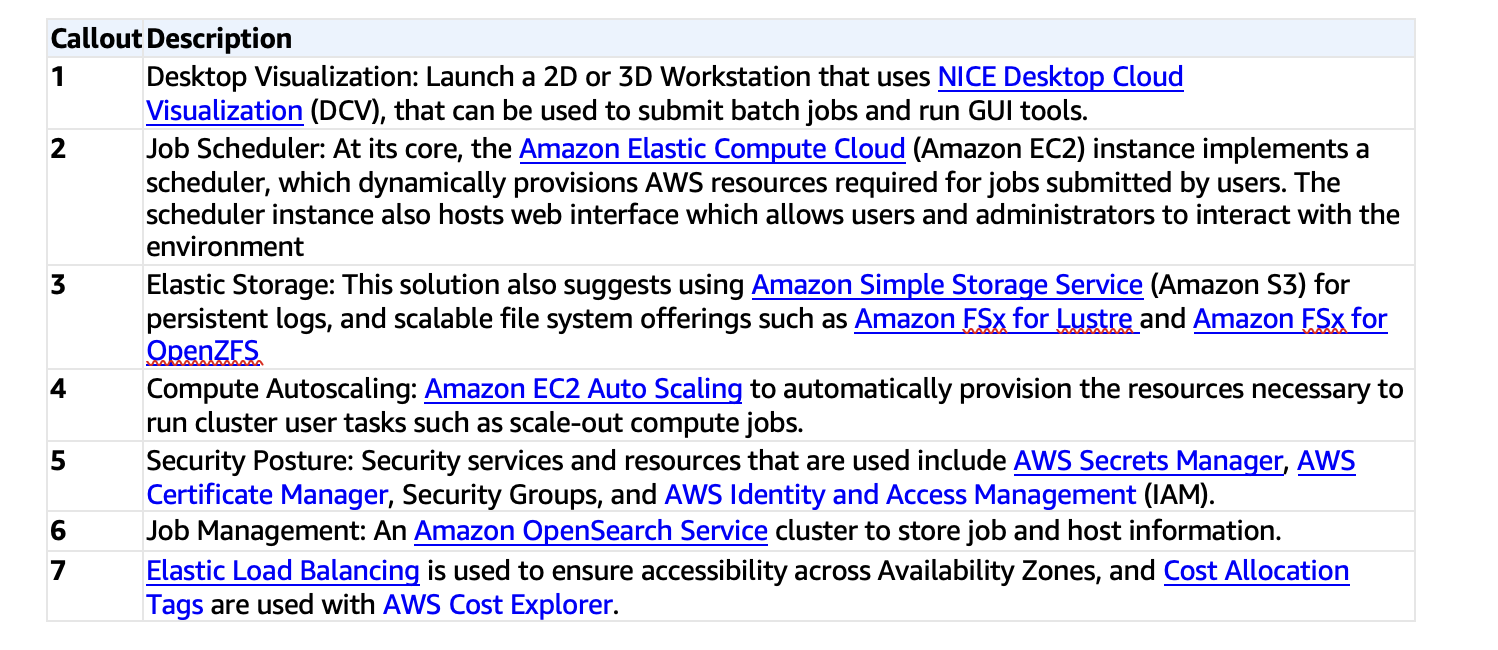
Open-Source Reference Architecture for Open-Source EDA Flows
After we have set up the NICE DCV based remote desktop instance for visualizing CAD applications, let’s look at a reference architecture that meets the critical needs of EDA workloads in a scalable way. The architecture features a large selection of compute resources; fast network backbone; unlimited storage; and budget and cost management directly integrated within AWS. The architecture also has a user interface (UI) for user & desktop management and automation tools that allows you to create your own queues, scheduler resources such as OpenPBS, Amazon Machine Images (AMIs), software, and libraries. This solution is designed to provide a production ready reference implementation as a starting point for deploying an AWS environment to run scale-out workloads.
The AWS Advantage:
AWS EC2 provides various instance types with different configurations of CPU, memory, storage, and networking resources so a user can tailor their compute resources to the needs of their application, those in the compute and memory-optimized categories are particularly suitable for chip design workloads. Developers can leverage AWS’ abundant compute and storage offerings that can be tailored for open-source EDA workloads to drive chip design innovation at a lower cost without compromising performance.
Compute Offerings:
Compute optimized instances such as C7g, C6i, M7g, M6i, M5zn, C5, and X2gd (and their disk variants) are appropriate for Regression tests, IP Characterization, Physical Synthesis, Digital, Analog and Mixed Signal Simulations. Memory optimized instancessuch as R7g, R7iz, X2iezn, and R6i/Hpc6id (and their disk variants) are well suited for physical design workloads such as Place & Route, Timing and Power Analysis, Design Rule Checking (DRC) and Batch Mode RTL simulations.
Shaping Compute to Workloads
With the broad selections of instances that designers can leverage for specific types of open-source EDA workloads. Figure 3 shows how different types of instances can map across both the Front-End Design and Verification, Back-end Physical Design and Verification and Product & Test domains of semiconductor design.

Storage Offerings:
For semiconductor design flows running at scale, storage can be the bottleneck that reduces job throughput. As the amount of data increases, the need to access that data across a fast-growing cluster means that the traditional on-prem filers eventually run out of storage space, or become bandwidth constrained by either the network or storage tier.
As a highly scalable alternative to NFS-based storage solutions,
Cloud-optimized semiconductor design workflows use a combination of Amazon FSx Family, Amazon EBS, Amazon EC2 instance store, and Amazon S3 to achieve extreme scalability at very low costs, without being bottlenecked by traditional storage systems.
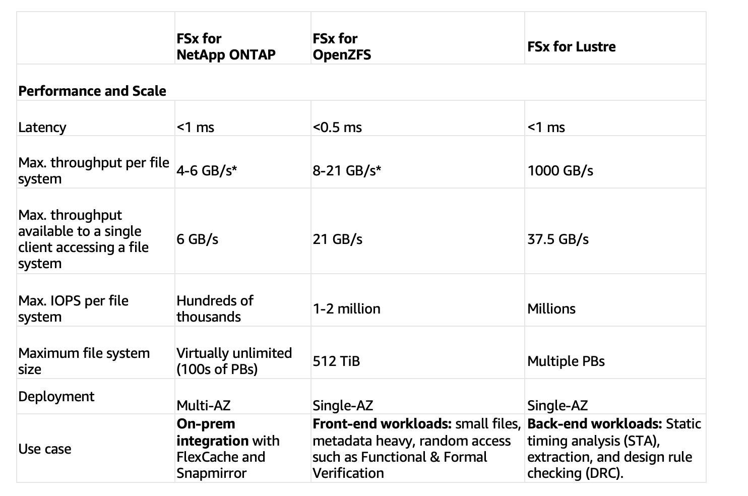
The following table provides detailed information for the different FSx storage types and the corresponding use case recommended for chip design workflows:
HPC powered by AWS:
Open-source High Performance Cluster (HPC) services such as AWS Parallel Cluster allows engineers and students to deploy and manage HPC services on AWS. With its simple graphical user interface (GUI), you can provision resources needed for your HPC applications in an automated and secure manner. AWS ParallelCluster is built on the popular open source CfnCluster project and is released via installing the GUI through an AWS CloudFormation template or the Python Package Index (PyPI). ParallelCluster’s source code is hosted on the Amazon Web Services repository on GitHub. AWS ParallelCluster is available at no additional charge, and you pay only for the AWS resources needed to run your applications.
Containers powered by AWS:
AWS container services make it easier to manage your underlying infrastructure. Nearly 80 percent of all containers in the cloud run on AWS today. Open-Source EDA provides chip designers compute platforms other than the traditional scheduler-based options and projects such as AutoTuner mentioned earlier, that leverage large Kubernetes cluster, can easily use managed container services from Amazon such as Amazon EKS. Below take provides a quick glance at some of the container services:

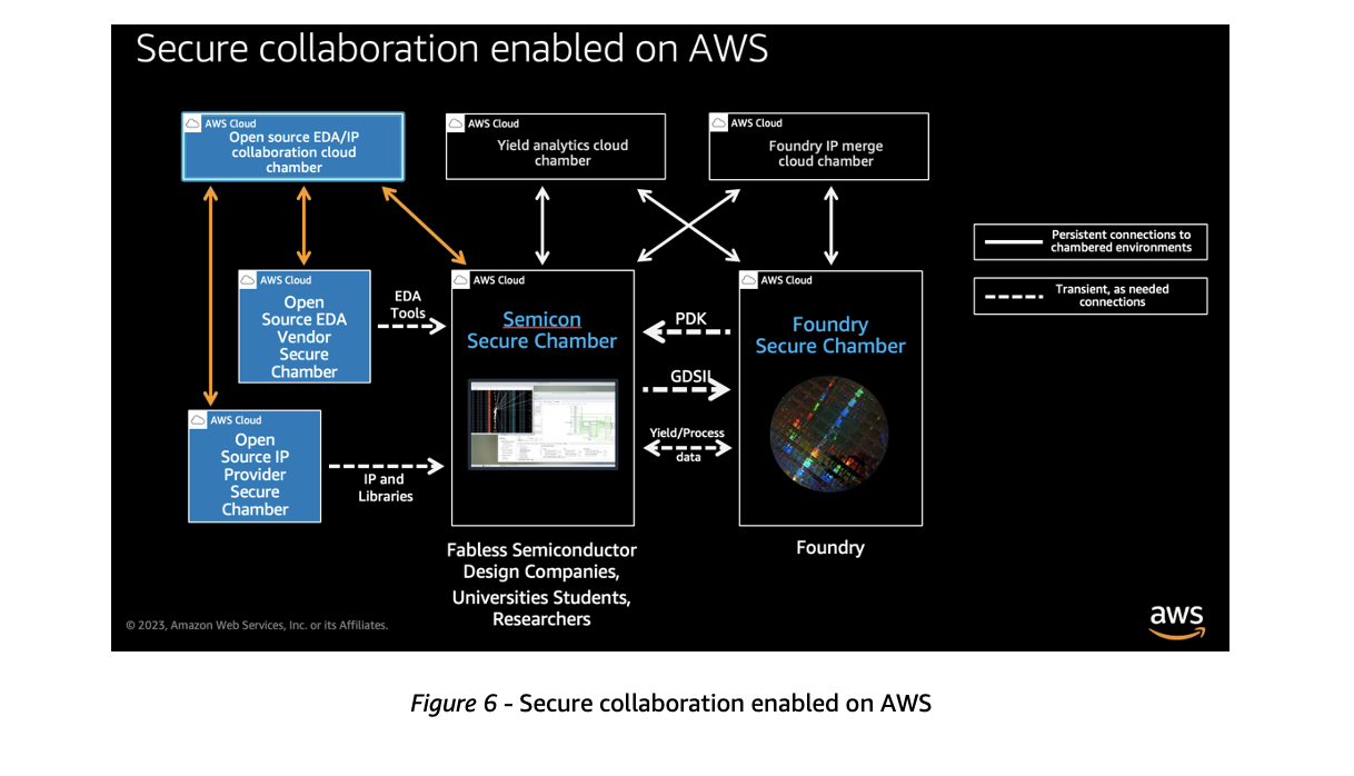
Secure Collaboration enabled on AWS:
Across the entire semiconductor industry, the need for collaboration is part of the design process, fabrication, and product manufacturing. AWS allows you to securely collaborate with research groups, third-party IP providers, open-source EDA developers, foundries, and contract manufacturers. For example, academic research groups for 2 or more universities might need to collaborate on a research paper outlining a novel algorithm for routing. Using AWS for collaboration makes it possible to segregate roles and data, lock down the environment to only authorized users, and monitor activity in the environment. Figure 6 graphically demonstrates how secure collaboration can be enabled on AWS.
Universities students & Researchers can collaborate in a secure environment with other academics and jointly innovate on open-source semiconductor designs. Using AWS services, 2 or more universities groups can setup a common design environment, complete with scalable compute & tailor-made storage as well as access to a wide array of other AWS services such as containers, ML/AI services and advanced data analytics capabilities.
Conclusion:
In this blog, we highlighted the recent efforts towards the progress of open-source EDA and how AWS can be used to run open-source EDA tools. The innovative open-source EDA projects, which include novel design algorithms, new EDA computing mechanisms and ML enhanced EDA, are a perfect match for cloud-based EDA design. We also highlighted how AWS can help specifically with EDA workloads. With a broad selection of compute instances across both x86 and ARM platforms, the high performance and scalable storage service and a comprehensive reference architecture.
We also discussed how AWS allows you to securely collaborate between several parties. Researchers, Universities students and professors can collaborate with other academics to innovate and develop the next generation of IP or SoC using open-source EDA software. Secure Collaboration chambers allows you to also collaborate with foundries and fine tune their final designs before fabrication.
In conclusion, Open-Source EDA ushers a new generation of EDA tools for today’s hyperscalers. Open-source EDA is well suited for the cloud, offering users benefits such as accessibility, scalability, collaboration, cost-effectiveness, and easy maintenance. By leveraging AWS for open-source, academia and startups can innovate quickly and research groups can collaborate securely and effectively. As next steps, we plan to develop implementation guides, white papers and reference architectures for running specific open-source EDA workloads on AWS.
Please visit the AWS Solutions for Semiconductor page for more information on how AWS can help you. For general information on open-source at AWS, click here.