AWS for Industries
Category: Semiconductor
Siemens PCBflow – Design validation for first-time-right manufacturing
Introduction First-time-right design is critical to cutting costs and reducing time to market, especially in today’s customized, high-demand environment. If you’re a Printed Circuit Board (PCB) designer or involved in PCB manufacturing, keep reading to learn more about Siemens PCBflow. PCBflow is a new cloud offering in the PCB Design for Manufacturing (DFM) domain, can […]

Accelerate Semiconductor Fab Transformation with AWS
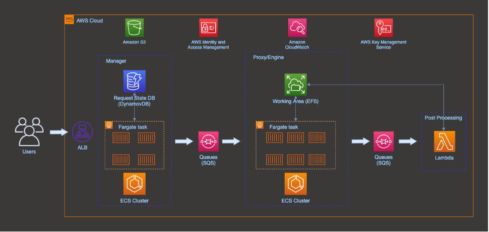
Introduction The high-volume manufacturing of semiconductor devices relies on complex wafer production and packaging processes, supported by a long list of specialized equipment manufacturers and materials suppliers. This heterogenous and globally distributed manufacturing supply chain must work closely with semiconductor design and verification teams. These teams create application-specific integrated circuits (ASICS) and systems-on-chip (SoC) to […]

Refactor Legacy Manufacturing Execution Systems into Event-Driven Microservices
Introduction Breaking the traditional methods of factory floor transformation using emerging cloud technology is often met with resistance. Transformation of manufacturers legacy Manufacturing Execution Systems, MES, commonly know as command and control systems is seen as a high-risk disruption. During the refactoring process, the potential of introducing a second of delay on factory floor is […]

Turning Price/Performance Upside Down: Ansys RedHawk-SC™ and Amazon Web Services
Introduction This blog discusses the insights Ansys and AWS were able to gain by scaling Ansys RedHawk-SC on the AWS Cloud. The joint investigation outlines how to right-size AWS compute and storage resource for optimal price/performance results while running at scale. By combining the capabilities of Ansys RedHawk-SC with being able to scale compute resources […]

AWS at DVCon US 2021 – Join us
Design and Verification Conference 2021 (DVCon) The Design and Verification Conference (DVCon) is the leading event covering the application of languages, tools and intellectual property for the design and verification of electronic systems and integrated circuits. Sponsored by Accellera Systems Initiative™, DVCon brings chip architects, design and verification engineers, and IP integrators the latest methodologies, […]

Listen to “AWS Industrial Insights” – A new podcast series for industrial business leaders
Introducing “AWS Industrial Insights” We are excited to launch a brand new podcast series, AWS Industrial Insights. In every episode, we interview visionary leaders from industrial companies to share their insights on technology, innovation, and leadership. This podcast is for industrial business leaders who are looking to make data-driven decisions and learn from those who’ve […]

Running Cadence JasperGold formal verification on AWS at scale
Introduction As the size and complexity of modern integrated circuits grow, semiconductor development teams are challenged to provide verification coverage for these larger, more complex chips with the same tight schedules. Formal Verification is an Electronic Design Automation (EDA) application commonly used by development teams to achieve this end. However, verification of modern Systems-on-Chip (SoC) designs increases […]

AWS for Industrial – Making it easy for customers to scale their industrial workloads on AWS
Increasingly, industrial customers across asset intensive industries such as manufacturing, energy, mining, transportation, and agriculture are leveraging new digital technologies to drive faster and more informed decisions in their industrial operations. ‘AWS for Industrial’ is a new initiative that features new and existing services and solutions from AWS and our Partners, which are built specifically […]
Secure collaboration with Altium on AWS
Introduction A forecast from International Data Corporate (IDC), a global market intelligence firm, predicts that by 2025 there will 55.9 billion connected devices, or “Internet of Things (IOT)”, worldwide. With these new devices, the need for Printed Circuit Board (PCB) design software will continue to grow. However, just having the right tools in the hands […]

Scaling Synopsys Proteus optical proximity correction on AWS
Introduction Photolithography is a key step in the manufacturing of semiconductor chips. Photolithography works by shining light (laser) through a pattern (mask) onto a silicon wafer with photosensitive coating (resist). This changes the properties of the coating allowing manufactures to chemically remove the parts of the coating based on the exposure or lack of exposure […]